
Menu:
Version:
December 6, 2019:
Revision: v1.1
The ZL2PD SugarCube Si5351 VFO
Just how small can you make a digital PLL VFO based on the Si5351a chip? I set out to demonstrate that it's feasible to design and build it in a volume close to that of a cube of sugar. Sweeten your tea or coffee with this new design!
IMPORTANT:
New upgraded software is now available for my SugarCube VFO. Click HERE to go to that page.
All of the information required to build the SugarCube hardware - the schematic, the PCB, wiring details, etc - is still located here on this page.If you've already built your SugarCube, the upgraded software is 100% compatible and adds a bunch of new features.
Introduction
A recent email chat about the Si5351a chip led me to claim in passing that it was probably possible these days to build a full-scale digital VFO in a matchbox. For those uncertain about the size of a matchbox, here’s what one looks like where I live.
2” x 1½ ” x ½”).
For some reason, this idea stayed in my head for a day or two. At that point, I realized it was probably equally feasible for a digital PLL VFO to fit in half that volume, and maybe an even less. However, to achieve something like that, it ultimately would depend on whether or not I could manage to squeeze all of the software necessary for a PLL chip and the matching compact display into the limited 8K flash memory of an ATtiny85.
To some reading this, reducing a VFO into such a small volume and with such a small microcontroller might appear impossible. Pointless, even, perhaps. However, from my perspective, almost all Si5351a VFOs out there, except for most of mine of course, seem to demand an Arduino with at least 32K of memory and a great deal of space. That tends to make these VFOs quite large. In turn, using them in many applications consequently becomes difficult, perhaps even impossible.
The display is also something of a critical issue. While one or two examples exist on the web showing the Si5351a being driven from an 8-pin ATtiny processor, such designs lack a useful or accurate display. Without an accurate easy to read display, how can you determine your operating frequency? To my thinking, that's a critical requirement. So, all of my VFOs must, and do, feature a useful frequency display of some type.
However, at the end of the day, could I design and built such a miniature PLL oscillator?. I just had to try this idea out. And, yes, it turned out to be perfectly feasible to build a well-featured digital PLL-based VFO in a volume fairly close to that of a common sugar cube. Really!
And for those readers unfamiliar with the size of sugar cube, here’s a picture of a few sugar cubes from our pantry alongside the new SugarCube VFO.
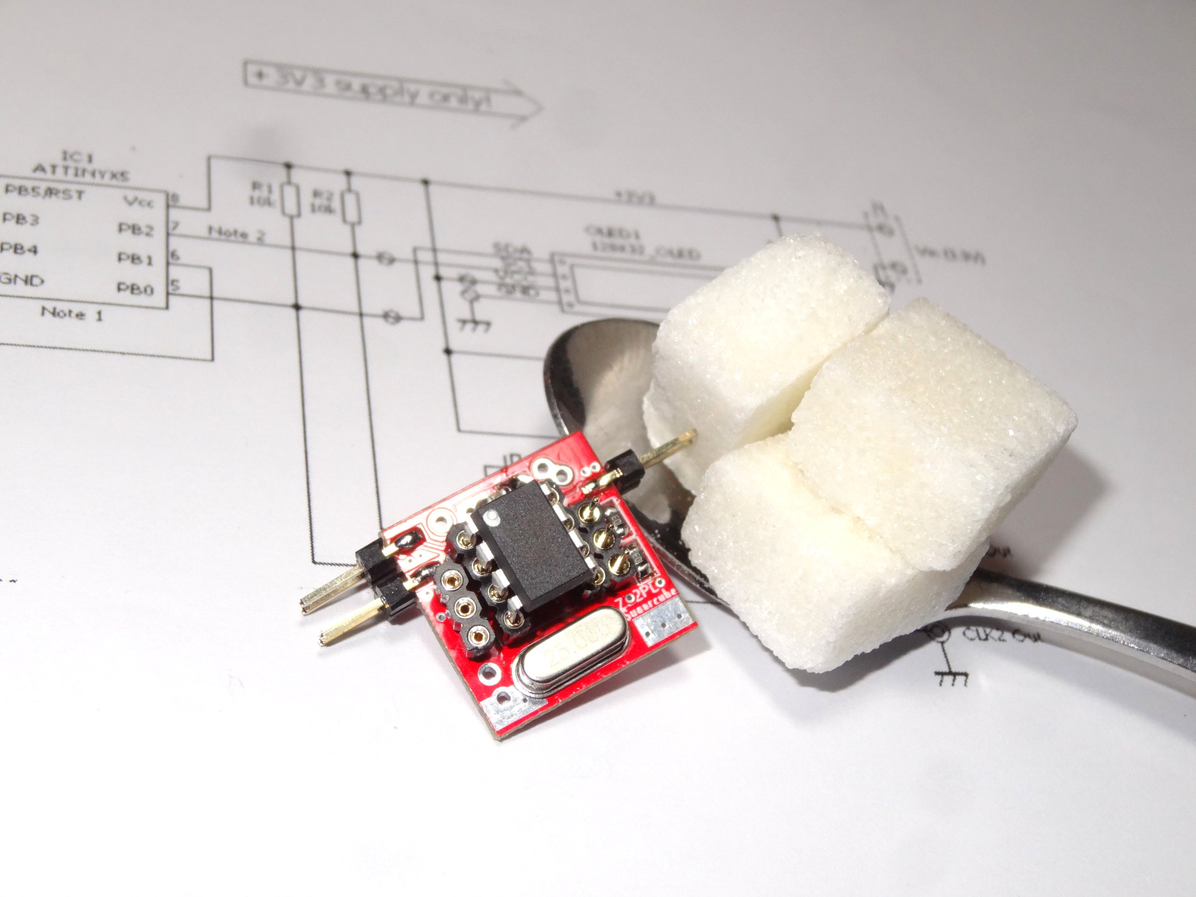
Figure 1 : The prototype Sugarcube VFO alongside a teaspoon with some real sugar cubes
But, hey! This is all fairly pointless if the resulting VFO has no features. What have I managed to squeeze inside the SugarCube VFO? I think you’ll agree, it’s quite a lot.
Features of the SugarCube VFO
In terms of the user interface, the SugarCube supports:- Digital tuning with a rotary encoder
- Tuning step size selection using the encoder’s integrated shaft pushbutton
- Two user pushbuttons – VFO selection (VFO A or VFO B) and Tuning Lock
- PTT input – The VFO can detect if you are in transmit or receive mode and set the VFO’s output frequencies accordingly (This equates to a third button which supports another feature, described later)
- Receiver signal strength/RF Power meter input – An analog voltage between 0 and 3.3VDC on this input is displayed on the bar-graph on the lower section of the OLED display
- Dual VFOs – Two VFOs are supported to allow, for example, rapid tuning between two bands, with each VFO (A and B) able to start on different programmable frequencies
- Wide VFO tuning range – The VFO typically supports any output frequency from 5kHz to 290MHz, the extreme frequencies being chip-dependent
- Quadrature
outputs - Output0 and Output1 of the Si5351a are phase shifted by 90
degrees between 3.5 MHz and somewhere above 200MHz (I don't have
suitable test gear to confirm the upper limit)
- User selectable tuning steps – 1Hz, 100Hz, 1, 10 and 100kHz, and 1MHz steps
- Tuning step indicator – A arrow on the OLED display points to the tuning step
- Tuning Lock – A lock button is supported for portable and mobile applications
- RSSI/Power meter – The display provides a bar-graph display along the lower edge to display the 0-3.3VDC input at pin 1 of the ATtiny85.
But wait, there's more:
- PTT input detection – Supports VFO IF offset operation where the receive VFO frequency is offset from the transmit frequency
- IF Offset – Programmable in software
- Standard 0.91” OLED display – Probably easier (and cheaper) to buy than some of the more specialised I2C LCDs used on my other VFOs, and it better compliments the smaller VFO hardware, I think

Figure 2 : The Sugarcube VFO's OLED display is small but very easy to read
(This
shows the typical display for a VHF version of the software. It shows
the operating frequency, the selected tuning step size, indicated by
the little arrow, the RSSI bargraph, constantly updated and flowing
across the display under the frequency display, and the icons for VFO
Lock, PTT and A (or B) VFO selection)
This compact 128 x 32 OLED I2C display uses a SSD1306 controller. It is more difficult to drive in software than the larger I2C-based alphanumeric displays I use in my other VFOs. However, it delivers three significant advantages – Size (obviously!), low cost, and it simplifies the VFO construction and installation.
Schematic and Description
The schematic diagram is shown below:
Figure 3 : The Sugarcube VFO has very few components
There’s really very little to the design, and equally little to describe.
The ATtiny85 microprocessor lies at the heart of the design. This little 8-pin powerhouse turns on, resets the Si5351a chip and the OLED display, then displays the startup configuration programmed in the ATtiny85 software. It then spends its life reading the switches and encoder, driving the display, and sending any new data to the si5351a via the I2C bus.
The pushbuttons generate different DC voltages on one of the ATtiny85's pins. In turn, these drive various software subroutines to produce the desired effect.
Everything is powered by the 3.3V supply. More about this shortly.
Software
As
is usual for my projects, my software has been written in Bascom, a
Basic-like language for the Atmel family of microcontrollers. It’s
easier to write and maintain than many other more popular software
languages. The compiler is reasonably efficient and, as you can see
from this example, the resulting code is quite compact. I’ve developed three different versions of the software as examples of a few of the possibilities with my new SugarCube VFO:
Version A: Standard HF VFO for typical transceiver with 8.87MHz IF
VFO A: Start: 14.100MHz (20m)
VFO B: Start: 3.650MHz (80m)
IF Offset: +8.867MHz
BFO/CIO: 8.870MHz
Output 0: VFO
Output 1: VFO – Quadrature
Output 2: BFO/CIO
Steps: 5Hz, 100Hz, 1kHz, 10kHz, 100kHz, 1MHz
VFO B: Start: 3.650MHz (80m)
IF Offset: +8.867MHz
BFO/CIO: 8.870MHz
Output 0: VFO
Output 1: VFO – Quadrature
Output 2: BFO/CIO
Steps: 5Hz, 100Hz, 1kHz, 10kHz, 100kHz, 1MHz
Version B: Standard HF VFO for typical transceiver which requires no IF offset
VFO A: Start: 14.100MHz (20m)
VFO B: Start: 3.650MHz (80m)
IF Offset: Nil
BFO/CIO: 8.870MHz (for test purposes)
Output 0: VFO
Output 1: VFO – Quadrature
Output 2: BFO/CIO
Steps: 5Hz, 100Hz, 1kHz, 10kHz, 100kHz, 1MHz
VFO B: Start: 3.650MHz (80m)
IF Offset: Nil
BFO/CIO: 8.870MHz (for test purposes)
Output 0: VFO
Output 1: VFO – Quadrature
Output 2: BFO/CIO
Steps: 5Hz, 100Hz, 1kHz, 10kHz, 100kHz, 1MHz
Version C: VHF Receiver VFO for receiver with 10.7MHz IF
VFO A: Start: 147.050MHz
VFO B: Start: 147.250MHz
IF Offset: +10.7MHz
BFO/CIO: 12.3450MHz (for test purposes)
Output 0: VFO
Output 1: VFO – Quadrature
Output 2: BFO/CIO
Steps: 5Hz, 100Hz, 1kHz, 25kHz, 100kHz, 1MHz
VFO B: Start: 147.250MHz
IF Offset: +10.7MHz
BFO/CIO: 12.3450MHz (for test purposes)
Output 0: VFO
Output 1: VFO – Quadrature
Output 2: BFO/CIO
Steps: 5Hz, 100Hz, 1kHz, 25kHz, 100kHz, 1MHz
I’ve provided the HEX code below in the download section for these three versions. Please note updated versions of the SugarCube software are available elsewhere on my website. More details about the operation of these three versions is found below. But first, I’ll explain how to build the SugarCube VFO.
Construction
All
the parts (and there really are not very many parts in this design!)
are all readily available at very attractive prices. At time of
writing, the SugarCube VFO can be built for (well) under $US10. I’ve designed a suitably tiny double-sided PCB for the SugarCube VFO. It uses a combination of SMD and through-hole parts. Here’s a close-up view of the top side of the 20 x 20mm PCB
It’s vital to mount the parts in the correct order when building the VFO.
Begin by fitting the Si5351a in the centre of the PCB on the top side of the PCB. I find using additional flux makes this task go smoothly. (The top side of the PCB is the side on which the text is written) You can see where the Si5351a is mounted in this view.

Figure 4 : The Si5351a sits underneath the ATtiny85 microcontroller
Then solder in the two SMD 0805-sized resistors on the top-side, and then the through-hole 100nF bypass capacitor from the REAR/UNDERSIDE of the PCB. Next, add the SMD 1206-size 1uF electrolytic on the TOP side. (If you prefer, it’s possible to fit the SMD capacitor first on the top side as I did here. Try to avoid filling the through-holes in the PCB pads with solder. Then install the through-hole capacitor from the top side as well. Both methods work. Your choice.)(Yes, if you look closely, you will see I’ve not fitted the second capacitor yet)
Now install the 25MHz crystal. Some crystals have metal cases which have minimal insulation around the crystal pins. These crystal cases can short out the PCB connections under the case. Some crystals are supplied with thin insulating pads for this purpose but most do not because they don’t have this problem. If you have a problem crystal, which you can check first by temporarily holding the crystal in place on the board (Don't solder it yet!) and checking for shorts with an ohmmeter, then there is a simple and effective solution.
Cut a small piece of transparent sticky tape and carefully push the pins of the crystal through the tape. You might find this easier to do if you use a sharp pin to make the holes in the tape first. Trim the tape to leave a 1mm excess tape around the case of the crystal. Then solder the crystal into the PCB. If you solder the crystal leads fairly quickly, the tape will successfully insulate the crystal from the PCB. If you need a longer time to solder the leads, use kapton (heat-proof) tape.
Now install the two 4-pin pin-strips to form the socket for the ATtiny85. The ATtiny85 will ultimately plug in over top of the Si5351a.
Now to the RF output connections. You can either fit two-pin 0.1” connectors or connect pieces of thin coaxial cable directly to the PCB pads..
Finally, install the wires for the encoder, switches and power, and connect then to the panel mounted items and to your power supply source as required.
Programming
For
those wanting to just program one of the HEX files to try out the
design first, just download the HEX files, grab a suitable programmer
(e.g. USBasp etc) and program your ATtiny85. Suitable GUI programmer
application software is available free via the internet. Examples
include Khazama and Extreme.Two steps are then required to program the ATtiny85 with the USBasp programmer – The flash memory must be programmed with the program software (One of the HEX files downloaded from the links below), and then the ATtiny85's fuses must also be correctly programmed. (Note: High=&H5f, Low=&He2) These configure the Tiny85 for each application.
IMPORTANT: If you intend to reprogram your ATtiny85 again later, perhaps to change the starting frequencies or the BFO/CIO frequency or the IF offset, then, before programming the chip again, these fuse settings require you to reset the fuses first. You will need to use a HV-type programmer for this. That’s all due to the Reset pin (pin 1) on the ATtiny85 being used in this design for the RSSI/RF power bar graph input.
I use an adapter board to program the ATtiny85 using most programmers such asthe very popular low cost USBasp. Such an adapter board is usually home-made. It consists of an 8-pin IC socket, a 6 pin 0.1” header strip to match the USBasp programmer's connector, all built using a scrap of prototyping board.
The circuit diagram for my adapter is shown below. The resistor and LED are optional. They were added to show me when power has been applied to the adapter board.

Figure 5 : Optional ATtiny85 programming adapter
In use, the ATtiny85 to be programmed goes into socket SKT1. The USBasp programmer is plugged into the 6 pin plug J2. 5V power comes from the programmer via J2 so J1 is normally unused)
If all of this remains a mystery for you, there are some helpful tutorials on this topic that can be found on the Adafruit and Instructables websites.
SugarCube VFO Wiring and Installation
Here’s
how to connect everything on the little SugarCube VFO. This diagram has
been drawn with all of the wiring and various parts spread out so you
can see all of the connections easily. In practice, the wiring consumes
minimal volume/space.
Figure 6 : The SugarCube VFO wiring is quite simple and easy to install
IMPORTANT: The 3.3V supply voltage to the VFO and OLED display MUST NOT be exceeded. It’s easy to supply the current of about 30mA required by the VFO from a small 78L33 TO-92 type regulator or from an existing 3.3V rail inside the equipment. There are some details on suggested methods described below.
I mounted a 3-way DIL machine pin socket into the PCB holes on the left hand side of the ATtiny85 and a three-way pin header in the three holes on the right hand side of the chip. This allowed me to wire to the panel parts using matching tiny connectors made from the matching pin strips. That allowed me to more easily route the wiring in the receiver, and in another transceiver.
Three pairs of two-pin “DuPont” 0.1” connectors can be directly soldered to the VFO output pads on the PCB and thin coax cables used to connect between these and the receiver or transceiver VFO/BFO inputs.
The PCB can be mounted into your equipment using solder tags soldered to the two square tinned pads at either corner of the lower edge of the VFO, or with double sided foam tape, or tack-soldering the little PCB in place.
Powering the SugarCube VFO
The
SugarCube VFO is supplied from 3.3V, a limit imposed by both OLED
display and the si5351a chip. It consumes about 30mA. There’s no 3.3V
regulator on the PCB to save space. It’s up to the user to provide a
suitable supply. Here are three ways to do it:

Figure 7 : A simple red LED can be used to supply 3.3V for the SugarCube VFO from a 5V rail
The first method is using a standard 3V3 regulator. Since the SugarCube VFO draws only 30mA, a small TO-92 packaged regulator works well.
The second possible approach uses two standard silicon diodes to drop about 1.4V. Hans Summers G0UPL uses this approach in his very popular QRX QRP transceiver. I found this method results in a somewhat higher supply voltage to the SugarCube VFO, typically 3.6V (i.e. 5V – 1.4V) which I think is too high for the Si5351a and this OLED display. However, it’s your choice.
The third method is the method I recommend. It’s cheap and simple. It uses a standard red LED, not one of the high efficiency red LEDs which drops more voltage. The standard red LED drops 1.6V which results in the right voltage for the VFO. You can see the LED cheerfully lit when operating. It turned out very well in my VHF receiver conversion.
Operation
When
power is applied, the SugarCube VFO will start on the frequency
programmed for VFO A +/- the programmed value of offset. Pressing the
VFO A/B button will change this frequency to that programmed for VFO B.
Pressing the button again will revert back to the other VFO frequency.Turning the rotary encoder tuning control will increase or decrease the selected VFO’s frequency. The tuning rate depends on the selected step size. This selection, changed by briefly pressing in the rotary encoder, is indicated by the status arrow on the upper edge of the OLED display.
Pressing the Lock button will retain the currently selected frequency and step size. A small padlock graphic symbol will appear at the upper right hand corner of the OLED display. Pressing the Lock button again will restore tuning and step selection functions, and the padlock icon will disappear.
In the case of Version A or B software, pressing and holding the PTT button will result in the SugarCube VFO entering the transmit mode. This removes any IF offset frequency from the CLK0 output. A small ‘T’ character will appear at the upper right hand corner of the OLED display to indicate this to the user. Releasing the PTT button will reapply any offset to the output frequency on CLK0 and the T character icon will disappear from the OLED display.
In Version C for the VHF receiver, a small 'S' character appears to indicate the receiver is monitoring the ("Simplex") frequency shown on the display rather than the VHF repeater output frequency (the "Duplex" offset frequency) which is 600kHz above or below the displayed frequency.
Configuring VFO Frequencies
The
starting frequencies for VFO A and VFO B are programmable in software.
For example, VFO A can be programmed to 14.100MHz and VFO B to
7.150MHz. When the power is applied, the SugarCube VFO will wake up in
receive mode (unless the PTT input is also grounded) with an output on
CLK0 as programmed for VFO A i.e. 14.100MHz +/- any programmed Offset.The CLK0 output signal on receive is the frequency shown on the display +/- any programmed offset. An offset is typically used when an IF stage is used in a receiver. For example, if your receiver has a 9.0MHz IF, VFO A in receive will output 14.100MHz + 9.000MHz = 23.100MHz (or 14.000-9.000 = 5.000MHz if low side injection is used). However, the display will show the receiver's operating frequency of 14.100MHz.
On transmit, the offset is often not required, so the VFO just outputs 14.100MHz on transmit. For applications where an IF offset is not required on eitehr receive or transmit, the value of the ‘Offset’ constant in the software should be set to 0 prior to compiling the code.
The CLK2 output signal generates the quadrature version of CLK0 i.e. Same frequency, 90 degrees phase shifted.
The CLK2 output signal generates the receiver’s Beat Frequency Oscillator (BFO) and transmitter’s Carrier insertion Oscillator (CIO) signal. This is usually set to a similar frequency to that of the IF (i.e. similar to that programmed as the Offset), but usually shifted slightly to locate it on the appropriate edge of the IF filter response.
For example, for a transceiver with an IF filter of 8.867MHz, the Offset would be programmed to 8.867MHz and the BFO/CIO, say, to 8.870kHz. (The exact BFO/CIO frequency to be programmed depends on the crstal filter shape and carrier tuning on the filter edge) Assuming a positive Offset, this would result in an initial startup frequency on CLK0 of (14.100+8.867) 22.967MHz. When the PTT input is grounded, the frequency of the 3.3Vpp square wave on CLK0 and CLK1 would change to 14.100MHz. CLK2 would remain the same in both receive and transmit modes, providing a 3.3Vpp square wave output at a frequency of 8.870MHz.
SugarCube VFO Application Example - A 2m VHF FM Receiver
I
have an old VHF receiver. It is a typical Motorola MC3362 single chip
receiver design first built perhaps 20 years ago. It was tuned with a
varicap tuned oscillator controlled by a multiturn pot on the front
panel. With only one chip, plus the LM386 audio amplifier, it was quite
compact. This was actually a kitset build, but a very typical example
of almost all such MC3362 VHF receivers. The receiver had been left on the shelf for years. There was no way to tell exactly where it was tuned - Somewhere between 144 and 148MHz.. And it drifted. On cold mornings, the local VHF amateur radio repeater would be in one place on the dial, but after a few minutes, it would gradually shift to a half-turn or more around the tuning dial. Then the sun might come out, shine on the receiver, and the receiver would then cheerfully drift off to an entirely new spot on the dial. The sun would go away, and so would the signal. Annoying.
I could have added a PLL oscillator back then, but that required the addition of a PLL chip, a controller, a VHF divider chip.... Given the small plastic enclosure I’d originally used for the receiver, adding a PLL system like that would have also probably have required a completely new case for the receiver. I never bothered.
That old receiver was an ideal target for my new SugarCube VFO. I built up one of the freshly arrived PCBs. Then it was the work of just a few minutes to remove the old varicap control and the old (large!) multi-turn tuning potentiometer, add a blocking capacitor, and replace the internal oscillator with the new SugarCube board. Here are the circuit changes:

Figure 8 : The changes to the original MC3362 circuit to add the SugarCube VFO are very simple
There was plenty of space on the front panel of the receiver for the new OLED display, and the VFO’s rotary encoder easily fitted into the location previously used by the old tuning potentiometer. The SugarCube VFO PCB was quickly mounted onto the old PCB in the receiver’s enclosure by tack-soldering it in place.
As a result, that receiver no longer drifts. It’s crystal-locked, effectively, thanks to the highly stable 25MHz crystal in my SugarCube VFO. Also, despite the small size of the display, and thanks to a little extra care with designing the digit graphics in the software I wrote, the display is quite easy to read, even for older visually-challenged users (like me!). I set up the tuning steps for VHF operation (i.e. 5kHz, 25kHz, 100kHz and 1MHz steps) and set the two VFOs to start up on two commonly used local 2m VHF repeater frequencies. Other channels in routine use here are available with a few extra clicks on the rotary encoder. Most importantly, the display accurately shows the receiver frequency.
Here’s a view of the inside of the modifed receiver. The wiring looks a bit messy. A bit more care with the layout would have made it look a bit nicer. Still, it demonstrates a fairly typical application using the SugarCube VFO. It’s quite hard to spot against the large VHF receiver PCB.

Figure 9 : The SugarCube VFO, display and controls were easy to add to an elderly VHF receiver
Signal Strength Meter Input
The
RSSI analog voltage input on the main circuit diagram shown earlier is
drawn with a 10k series resistor in the schematic. It is not present on
the PCB. I included it on the schematic to show a simple way to protect
the RSSI input but, in practice, individual requirements will determine
the specific arrangement used. Regardless of the approach, DO NOT EXCEED 3.3VDC ON PIN 1!!!Here’s one example of how to use this input.
I used this input on my VHF receiver to add a rather basic signal strength display. The MC3362 has a pin (pin 10) which can produce a voltage output with a suitable resistor for use with a signal strength meter. It can give a very accurate RSSI display. However, many FM VHF receiver designs, including my old receiver, use it to drive a squelch control. Sadly, that meant I could not use it to produce the desired accurate receiver signal strength meter display on my receiver.
As an alternative, and more to demonstrate the use of the RSSI input, I added a simple audio level interface to my receiver. The resulting front panel OLED display shows the approximate level of the demodulated FM speech using the RSSI input. It’s not an accurate display of anything, really, but it looks nice driving the display RSSI. Here’s the simple additional circuit I fitted.

Figure 10 : The RSSI input was driven using this added amplifier/rectifier circuit
The audio signal is amplified using Q1 and the resulting audio level is rectified with D1 and D2. This voltage is smoothed with C3 and discharged by R3. The result is a pleasing audio level meter display. It was built on a scrap of prototyping board and hot glued in place on the receiver PCB. Yes, it was not very pretty, but it’s on the inside and out of sight.
Final Thoughts
Here’s
my upgraded VHF receiver with its SugarCube VFO in action on my desk.
It’s quite compact - The front panel measures about 70 x 50mm. I’ve
been listening to local VHF repeater traffic going to and fro while
I’ve been writing much of this.
Figure 11 : The VHF recevier in use on my desk
Of course, the SugarCube is likely to be equally useful for a wide variety of other purposes. I hope you find it as useful and easy to use as I do.
Downloads
 Software
– Three HEX files are available here. See above text for details of
each version.
Software
– Three HEX files are available here. See above text for details of
each version. - Version A: Standard HF VFO for typical 8.87MHz IF transceiver
- Version B: Standard HF VFO for a transceiver with no IF offset or simple RF oscillator
- Version C: VHF Receiver VFO for receiver with 10.7MHz IF
PCB layout – The set of Gerber files for this little PCB VHF receiver front panel layout : Just an example to show the approximate positioning of the pushbuttons and their labels for such an application...
Questions? Send me an email. I'll try my best to answer as soon as I can. However, my (paid) work takes priority so it may take a couple of days....or longer if I'm travelling or sleeping.
Special versions? Well, feel free to ask, but it's unlikely I'll have the time to do any special version of the software just for you. However, if your idea interests me and if it has potentially wider application for a number of other users, and if I have some time, I'll have a look at it. Then I'll probably include it here with the others.
Want to go back to the main page? Click here to return directly.